Every gadget we use today, from our smartphones to our laptops, owes its existence to a complex, sophisticated process known as semiconductor testing. These tiny components form the backbone of our digital world, and their testing and validation are critical to ensuring the quality and functionality of electronic devices. This blog post will take you on a fascinating journey exploring the role of test wafers in the realm of semiconductor testing – from the nascent stages of prototyping to the final stages of production.
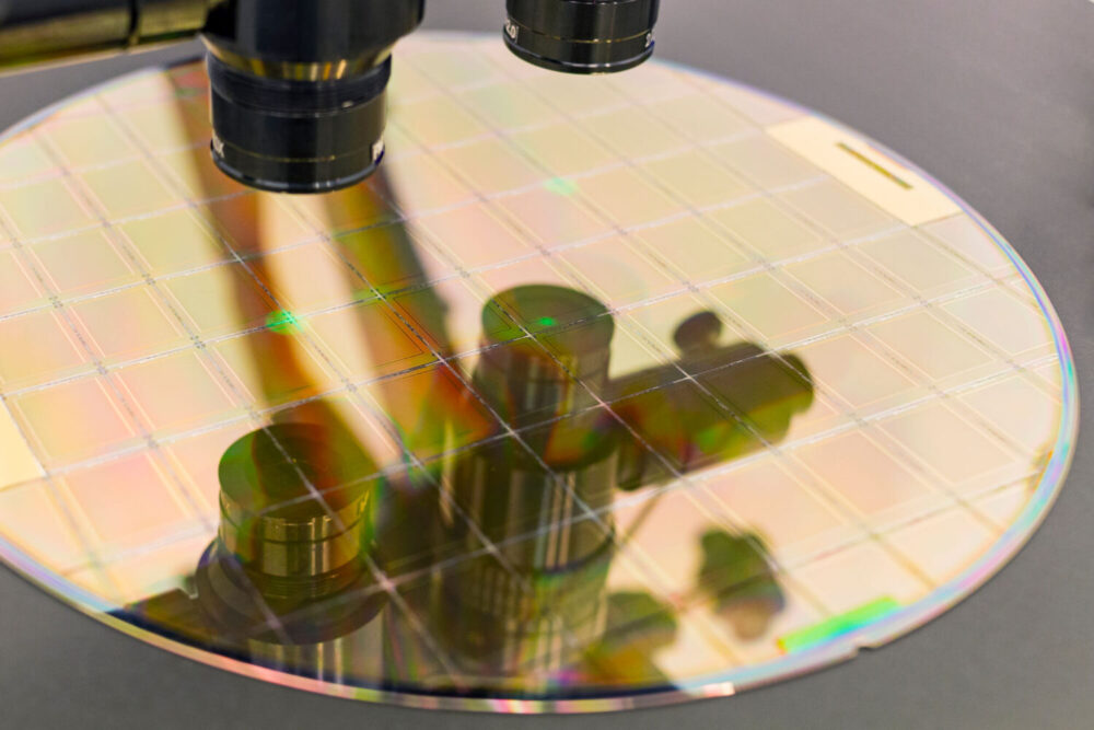
Understanding Semiconductor Testing
Source: waferworld.com
In the world of electronic devices, semiconductor testing is a critical quality assurance process. It ensures the functionality and reliability of integrated circuits (ICs), which form the heart of any electronic device. Semiconductor testing involves several stages: from initial design and prototyping to final production. One vital component of this process is the test wafer – an essential tool used to evaluate and optimize the performance and reliability of semiconductor devices.
The Role of Test Wafers in Prototyping
At the prototype stage, test wafers serve as indispensable tools for assessing the viability of new designs. These blank canvases, designed to mimic the electrical properties of actual semiconductors, provide engineers with a platform to evaluate the performance and functionality of their creations.
By subjecting test wafers to a range of operating conditions and rigorous testing, engineers can gauge how well the design meets intended specifications. This iterative process of testing, refining, and optimizing is driven by the critical feedback provided by test wafers, informing subsequent design improvements and ultimately paving the way for successful production.
Test Wafers in Process Development
In the realm of process development, test wafers play a pivotal role in fine-tuning fabrication techniques. These wafers closely emulate the characteristics of actual production wafers, enabling engineers to optimize processes such as photolithography, etching, and deposition. By experimenting with different parameters and configurations on test wafers, engineers can identify the most efficient and effective methods to maximize yield and ensure high-quality semiconductor production.
Test wafers provide a reliable platform for process optimization, allowing engineers to make informed decisions that streamline production, reduce defects, and meet the demanding standards set by the industry and consumers alike.
Characterization and Reliability Testing

Source: waferworld.com
Characterization and reliability testing are the next stages where test wafers prove their worth. Here, they are subjected to rigorous testing, including electrical, thermal, and mechanical evaluations, to characterize the device’s behavior under various conditions and ensure it’s reliable over its intended lifetime. This rigorous scrutiny helps guarantee that the ICs will perform consistently in real-world applications, providing the reliability that consumers and industries demand.
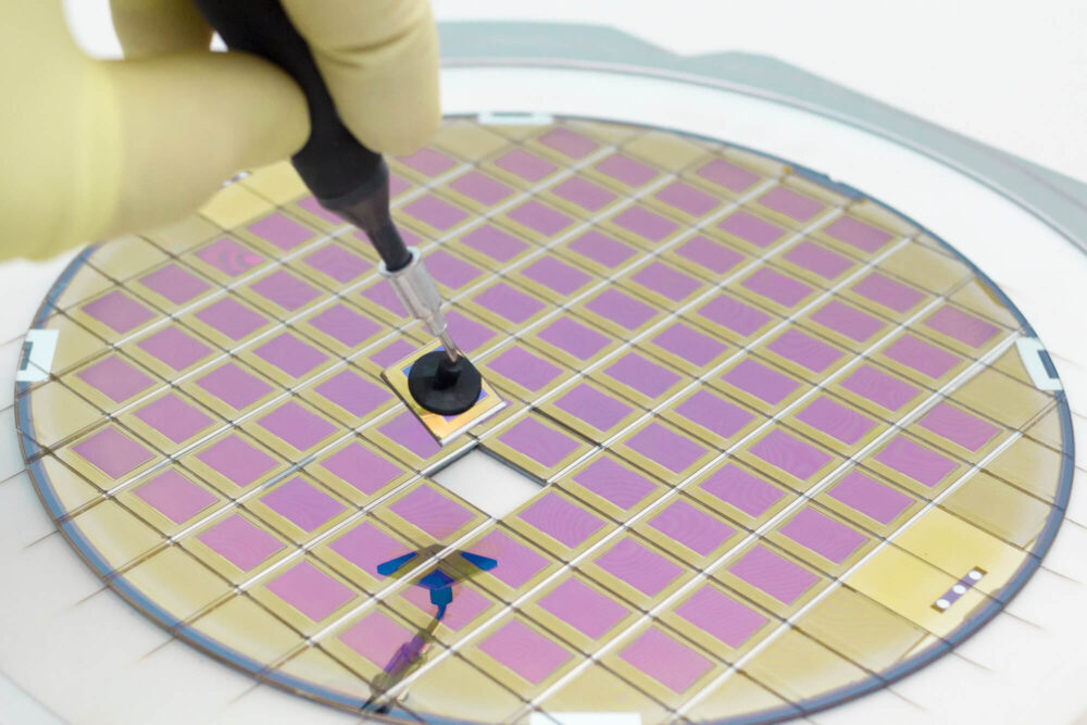
Test Wafers in Yield Analysis and Fault Diagnosis
Test wafers are also integral to yield analysis and fault diagnosis. They help identify and diagnose manufacturing defects and process variations that could affect yield—the percentage of functional chips in a wafer. By pinpointing these issues, test wafers help optimize production efficiency, minimize waste, and reduce costs, making the manufacture of semiconductor devices more profitable and sustainable.
Final Production Testing
In the final production testing phase, test wafers continue to play a crucial role in ensuring the quality and performance of semiconductor devices. These wafers are employed to verify the functionality, performance, and reliability of the finished products before they are released into the market.
Comprehensive testing is conducted to ensure that the integrated circuits (ICs) meet all their specifications and operate flawlessly when integrated into electronic devices. This rigorous testing process guarantees that end-users receive high-quality, reliable products that perform as intended.
As you can presume, the final production testing is essential. We are talking about the part of the process that will determine the prototype at hand. We are talking about a procedure that takes a lot of time, but it is absolutely necessary to avoid potential money waste.
When clients are not satisfied with the product, they want their money back, which leads to a drop in trust. We are talking about all the industries and companies, not just this one. With that in mind, it is essential to be especially careful in this process. That is why it is important to find rapid prototyping services that are reliable.
Test Wafer Design and Fabrication
The design and fabrication of test wafers is a meticulous process that requires expertise and precision. Test wafers are specifically designed to accurately simulate the characteristics of the actual semiconductor devices they represent.
Materials, designs, and patterns are carefully selected to ensure that the test wafers closely emulate the behavior and performance of the final products. This attention to detail and the creation of test wafers that mirror real-world conditions allow for accurate evaluation and assessment of the devices’ functionality and performance.
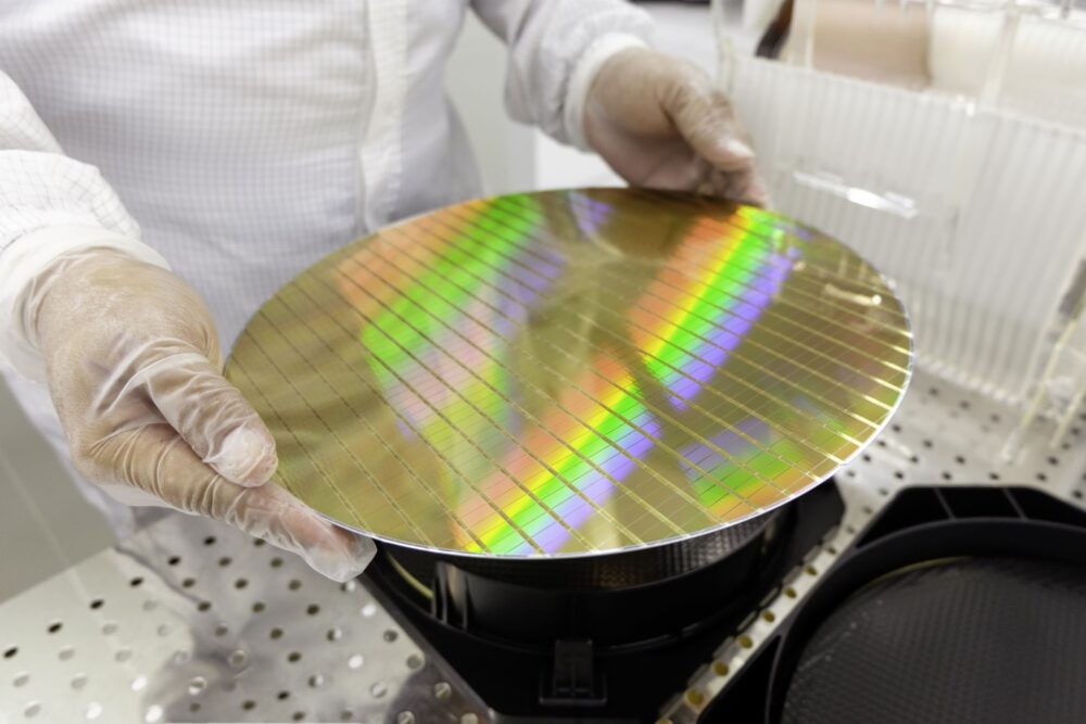
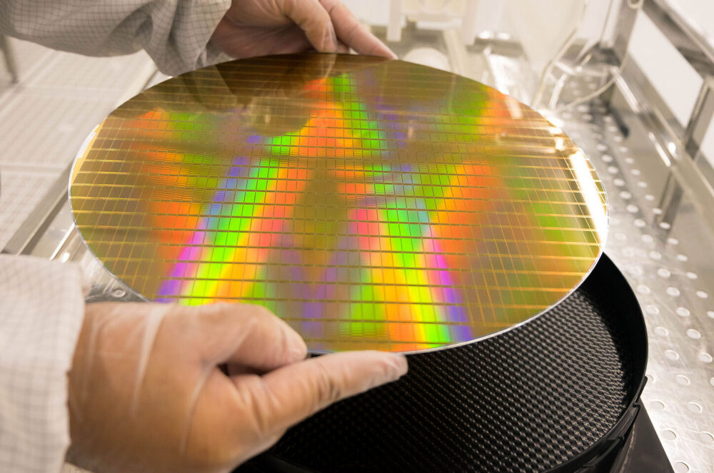
Handling and Logistics
Source: michigansthumb.com
Throughout their journey, proper handling of test wafers is of paramount importance to maintain their integrity and prevent any contamination or damage that could compromise their reliability and performance. Specialized equipment and cleanroom environments are employed to ensure a controlled and contamination-free environment for handling and processing test wafers.
Strict protocols are followed to protect the wafers from external particles, static electricity, and other potential sources of contamination. By maintaining the pristine condition of the test wafers, accurate and reliable test results can be obtained, enabling technicians and engineers to make informed decisions during the semiconductor testing process.
Effective test wafer handling and logistics not only safeguard the integrity of the wafers but also contribute to the overall efficiency and accuracy of the semiconductor testing procedures.
Adhering to stringent protocols and utilizing advanced handling techniques minimize the risk of errors and ensure that the test wafers provide reliable data for analysis and decision-making.
This meticulous approach to test wafer handling underscores the importance of maintaining the highest standards of quality and precision throughout the semiconductor testing journey.
Advancements and Innovations
Source: techpowerup.com
Test wafer technology is continuously evolving, with advancements like wafer-level testing, advanced packaging techniques, and miniaturized test structures leading the way. These innovations are transforming the testing landscape, enabling more efficient and accurate assessments of semiconductor devices.
Quality Control
Test wafers play a pivotal role in quality control. They help identify potential production defects, enabling their prevention and the production of high-quality ICs. The importance of stringent quality control in semiconductor testing cannot be overstated—it’s the linchpin that ensures every chip meets the highest standards of performance and reliability.
Conclusion
Test wafers are the unsung heroes of the semiconductor industry. From prototyping to final production, they play a crucial role in the testing journey, helping ensure that every semiconductor device is reliable, functional, and ready to power the digital devices we depend on. As technology continues to evolve and demand for electronic devices grows, the role of test wafers in maintaining the quality and performance of semiconductors will remain as vital as ever.